

Filter
Showing all 13 resultsSorted by latest
Sort:
Show:
| Parameter | Specification |
|---|---|
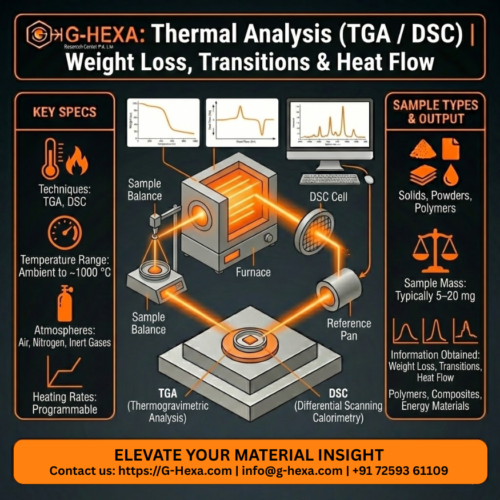
| Techniques | Thermogravimetric Analysis (TGA), Differential Scanning Calorimetry (DSC) |
| Temperature Range | Ambient to ~1000 °C (system dependent) |
| Atmospheres | Air, nitrogen, inert gases |
| Heating Rates | Programmable |
| Sample Type | Solids, powders, polymers |
| Sample Mass | Typically 5–20 mg |
| Information Obtained | Weight loss, transitions, heat flow |
| Typical Use Cases | Polymers, composites, energy materials |

| Parameter | Specification |
|---|---|
| Technique | FTIR Spectroscopy |
| Measurement Modes | ATR, transmission, reflectance |
| Spectral Range | ~400–4000 cm⁻¹ |
| Sample Type | Solids, powders, films, liquids |
| Sample Preparation | Minimal |
| Quantitative Capability | Semi-quantitative |
| Information Obtained | Functional groups, chemical bonding |
| Typical Use Cases | Polymers, coatings, organics, composites |
| Parameter | Specification |
|---|---|
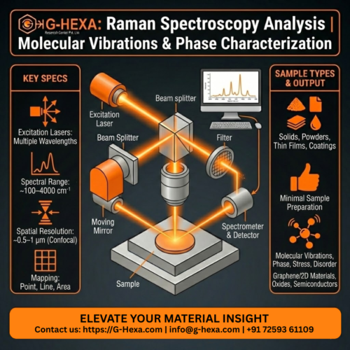
| Technique | Raman Spectroscopy |
| Excitation Lasers | Multiple wavelengths (system dependent) |
| Spectral Range | ~100–4000 cm⁻¹ |
| Spatial Resolution | ~0.5–1 µm (confocal) |
| Mapping | Point, line, and area mapping |
| Sample Type | Solids, powders, thin films, coatings |
| Sample Preparation | Minimal |
| Information Obtained | Molecular vibrations, phase, stress, disorder |
| Typical Use Cases | Graphene/2D materials, oxides, semiconductors |
| Parameter | Specification |
|---|---|
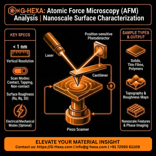
| Technique | Atomic Force Microscopy (AFM) |
| Imaging Resolution | Nanometer to sub-nanometer (vertical) |
| Scan Modes | Contact, Tapping, Non-contact |
| Scan Area | Up to ~100 × 100 µm² (system dependent) |
| Height Sensitivity | < 1 nm |
| Surface Roughness | Ra, Rq, 3D roughness metrics |
| Electrical Modes | C-AFM (optional) |
| Mechanical Mapping | Force modulation / phase imaging (optional) |
| Sample Type | Conductive and non-conductive solids, thin films |
| Sample Preparation | Minimal (flat, clean surface preferred) |
| Information Obtained | Topography, roughness, nanoscale surface features |
| Typical Use Cases | Thin films, coatings, semiconductors, polymers |
| Parameter | Specification |
|---|---|
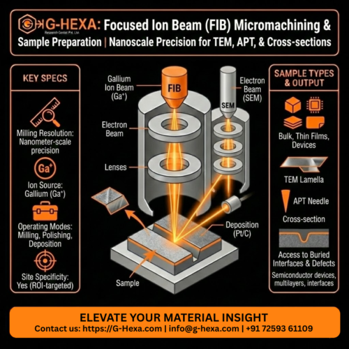
| Technique | Focused Ion Beam (FIB) |
| Ion Source | Gallium (Ga⁺) ion beam |
| Milling Resolution | Nanometer-scale precision |
| Operating Modes | Milling, polishing, deposition |
| Imaging Support | SEM-assisted navigation |
| Deposition | Protective layers (Pt / C) |
| Sample Geometry | Bulk, thin films, devices |
| Site Specificity | Yes (ROI-targeted) |
| Sample Preparation | TEM lamella, APT needle, cross-section |
| Information Enabled | Access to buried interfaces and defects |
| Typical Use Cases | Semiconductor devices, multilayers, interfaces |
| Parameter | Specification |
|---|---|
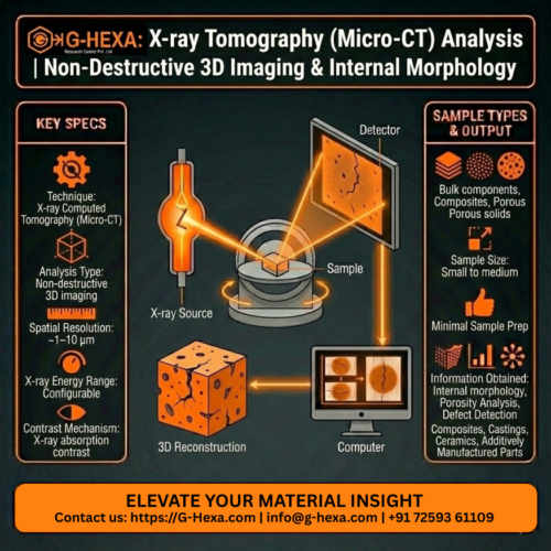
| Technique | X-ray Computed Tomography (Micro-CT) |
| Analysis Type | Non-destructive 3D imaging |
| Spatial Resolution | ~1–10 µm (system and sample dependent) |
| X-ray Energy Range | Configurable (material dependent) |
| Contrast Mechanism | X-ray absorption contrast |
| Volume Reconstruction | Full 3D volumetric datasets |
| Porosity Analysis | Volume %, pore size and distribution |
| Defect Detection | Cracks, voids, inclusions |
| Sample Type | Bulk components, composites, porous solids |
| Sample Size | Small to medium components (size dependent) |
| Sample Preparation | Minimal (mounting only) |
| Information Obtained | Internal morphology, density variation, defect distribution |
| Typical Use Cases | Composites, castings, ceramics, additively manufactured parts |
| Parameter | Specification |
|---|---|
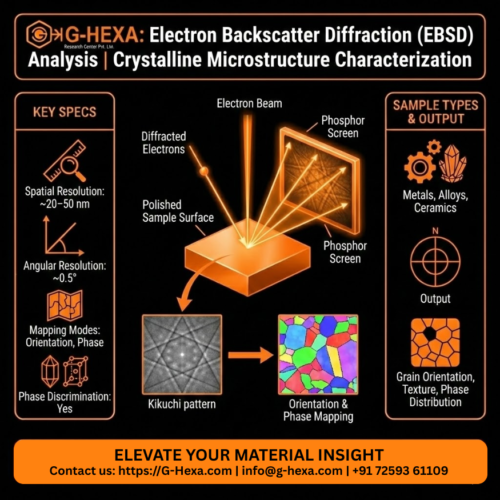
| Technique | Electron Backscatter Diffraction (EBSD) |
| Operating Platform | FESEM-based EBSD system |
| Spatial Resolution | ~20–50 nm (material and setup dependent) |
| Angular Resolution | ~0.5° |
| Mapping Modes | Orientation mapping, phase mapping |
| Grain Analysis | Grain size, grain boundary character |
| Texture Analysis | Pole figures, inverse pole figures |
| Phase Discrimination | Yes (crystalline phases) |
| Sample Type | Metals, alloys, ceramics, crystalline materials |
| Sample Surface | Highly polished, strain-free surface required |
| Sample Preparation | Precision grinding, polishing, vibratory polishing |
| Information Obtained | Grain orientation, texture, phase distribution |
| Typical Use Cases | Metallurgy, ceramics, thin films, failure analysis |
| Parameter | Specification |
|---|---|
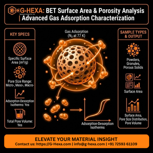
| Technique | BET Surface Area Analysis |
| Measurement Principle | Gas adsorption (typically N₂ at 77 K) |
| Specific Surface Area | m²/g |
| Pore Size Range | Micro-, meso-, and macro-porosity |
| Pore Size Analysis | BJH / DFT methods (optional) |
| Total Pore Volume | Yes |
| Adsorption–Desorption Isotherms | Yes |
| Sample Type | Powders, granules, porous solids |
| Sample Mass | Typically 50–500 mg (material-dependent) |
| Degassing | Vacuum / temperature-controlled degassing |
| Information Obtained | Surface area, pore size distribution, pore volume |
| Typical Use Cases | Catalysts, energy materials, porous ceramics, oxides |
| Parameter | Specification |
|---|---|
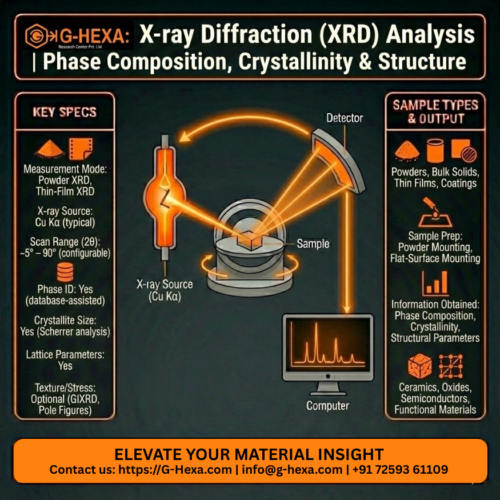
| Technique | X-ray Diffraction (XRD) |
| Measurement Mode | Powder XRD, Thin-Film XRD |
| X-ray Source | Cu Kα (typical) |
| Scan Range (2θ) | ~5° – 90° (configurable) |
| Phase Identification | Yes (database-assisted) |
| Crystallite Size | Yes (Scherrer analysis) |
| Lattice Parameters | Yes |
| Texture / Orientation | Optional (GIXRD, pole figures) |
| Stress / Strain | Optional |
| Sample Type | Powders, bulk solids, thin films, coatings |
| Sample Preparation | Powder mounting, flat-surface mounting |
| Information Obtained | Phase composition, crystallinity, structural parameters |
| Typical Use Cases | Ceramics, oxides, semiconductors, functional materials |
| Parameter | Specification |
|---|---|
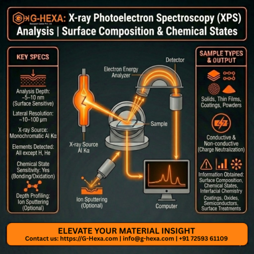
| Technique | X-ray Photoelectron Spectroscopy (XPS) |
| Analysis Depth | ~5–10 nm (surface sensitive) |
| Lateral Resolution | ~10–100 µm (instrument-dependent) |
| X-ray Source | Monochromatic Al Kα (typical) |
| Elements Detected | All elements except H and He |
| Chemical State Sensitivity | Yes (bonding and oxidation states) |
| Quantification | Atomic % composition |
| Depth Profiling | Ion sputtering (optional) |
| Sample Type | Solids, thin films, coatings, powders |
| Sample Conductivity | Conductive and non-conductive (charge neutralization supported) |
| Information Obtained | Surface composition, chemical states, interfacial chemistry |
| Typical Use Cases | Coatings, oxides, semiconductors, surface treatments |
| Parameter | Specification |
|---|---|
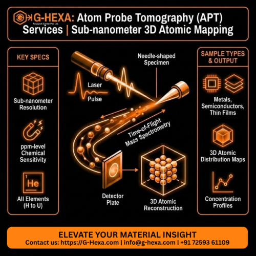
| Technique | Atom Probe Tomography (APT) |
| Spatial Resolution | Sub-nanometer (3D atomic mapping) |
| Chemical Sensitivity | ppm-level |
| Detection Method | Time-of-Flight Mass Spectrometry |
| Analysis Mode | Laser-pulsed or Voltage-pulsed |
| Analysis Volume | Needle-shaped specimen (~50–100 nm tip radius) |
| Sample Type | Metals, semiconductors, thin films, multilayers |
| Sample Geometry | Sharp needle specimen |
| Sample Preparation | FIB-based site-specific needle preparation |
| Information Obtained | 3D atomic distribution, dopant clustering, interface chemistry |
| Data Output | Atomic maps, concentration profiles, compositional statistics |
| Typical Use Cases | Semiconductor nodes, interfaces, diffusion and segregation analysis |
| Parameter | Specification |
|---|---|
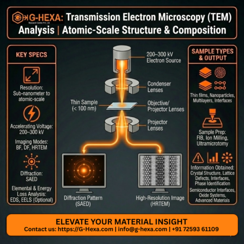
| Technique | Transmission Electron Microscopy (TEM) |
| Resolution | Sub-nanometer to atomic-scale |
| Accelerating Voltage | Typically 200 – 300 kV |
| Imaging Modes | Bright Field (BF), Dark Field (DF), HRTEM |
| Diffraction | Selected Area Electron Diffraction (SAED) |
| Elemental Analysis | EDS / EDX (optional) |
| Energy Loss Analysis | EELS (optional) |
| Sample Thickness | < 100 nm (electron transparent) |
| Sample Type | Thin films, nanoparticles, multilayers, interfaces |
| Sample Preparation | FIB lamella, ion milling, ultramicrotomy |
| Information Obtained | Crystal structure, lattice defects, interfaces, phase identification |
| Typical Use Cases | Semiconductor interfaces, oxide systems, advanced functional materials |
| Parameter | Specification |
|---|---|
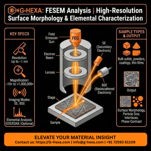
| Technique | Field Emission Scanning Electron Microscopy (FESEM) |
| Resolution | Up to ~1 nm (instrument-dependent) |
| Magnification Range | ~10× to >1,000,000× |
| Accelerating Voltage | 0.5 – 30 kV |
| Imaging Modes | Secondary Electron (SE), Backscattered Electron (BSE) |
| Elemental Analysis | EDS / EDAX (optional) |
| Sample Type | Bulk solids, powders, coatings, thin films |
| Sample Conductivity | Conductive or non-conductive (coating supported) |
| Sample Preparation | Mounting, coating, cross-sectioning (optional) |
| Information Obtained | Surface morphology, particle size, interfaces, phase contrast |
| Typical Use Cases | Failure analysis, coating evaluation, semiconductor inspection |