
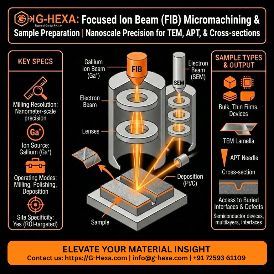
Focused Ion Beam (FIB) Micromachining & Sample Preparation
| Parameter | Specification |
|---|---|
| Technique | Focused Ion Beam (FIB) |
| Ion Source | Gallium (Ga⁺) ion beam |
| Milling Resolution | Nanometer-scale precision |
| Operating Modes | Milling, polishing, deposition |
| Imaging Support | SEM-assisted navigation |
| Deposition | Protective layers (Pt / C) |
| Sample Geometry | Bulk, thin films, devices |
| Site Specificity | Yes (ROI-targeted) |
| Sample Preparation | TEM lamella, APT needle, cross-section |
| Information Enabled | Access to buried interfaces and defects |
| Typical Use Cases | Semiconductor devices, multilayers, interfaces |
Payment. Payment upon receipt of goods, Payment by card in the department, Google Pay, Online card, -5% discount in case of payment
Warranty. The Consumer Protection Act does not provide for the return of this product of proper quality.
Description
Advanced Focused Ion Beam service for site-specific micromachining, cross-sectioning, and high-precision sample preparation. FIB enables controlled material removal at nanometer scale, making it indispensable for correlative microscopy, interface analysis, and advanced characterization workflows.
Key Applications
-
Site-specific TEM lamella preparation
-
APT needle preparation
-
Cross-sectioning of thin films and devices
-
Failure analysis and defect isolation
-
Interface and multilayer exposure
Specifications
Sample Preparation Capabilities
-
TEM lamella preparation (plan-view & cross-sectional)
-
APT needle fabrication with site-specific targeting
-
Cross-sectioning of devices, coatings, and stacks
-
Low-damage polishing for high-quality downstream analysis
-
(FIB preparation quality directly determines TEM, APT, and EBSD data reliability.)
Deliverables
-
Prepared TEM lamella or APT needle specimens
-
High-precision cross-section images
-
Site-specific documentation and imaging
-
Preparation notes aligned with downstream analysis requirements
Who Should Use This Service
-
Semiconductor device and process engineers
-
Advanced materials and interface researchers
-
Failure analysis and reliability teams
-
Organizations requiring correlative TEM / APT / EBSD analysis
Important Note
FIB is a destructive, ion-based technique.
Careful parameter selection and preparation strategy are essential to minimize damage and artefacts. Our team evaluates each sample and defines the optimal preparation route prior to execution.


Reviews
There are no reviews yet.