
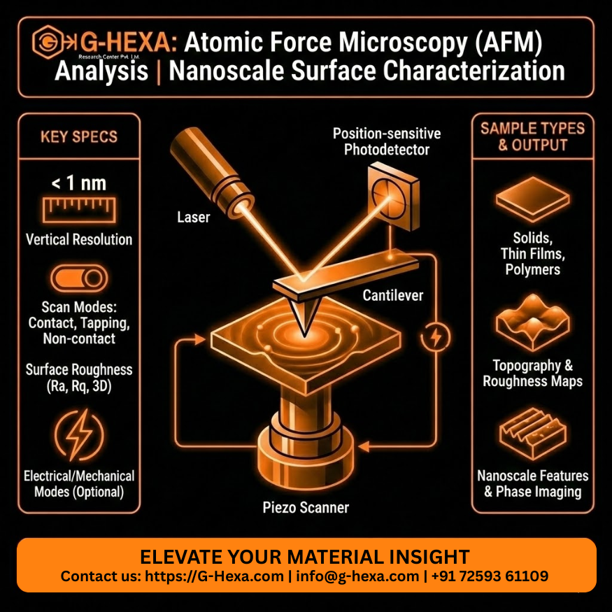
Atomic Force Microscopy (AFM) Analysis
| Parameter | Specification |
|---|---|
| Technique | Atomic Force Microscopy (AFM) |
| Imaging Resolution | Nanometer to sub-nanometer (vertical) |
| Scan Modes | Contact, Tapping, Non-contact |
| Scan Area | Up to ~100 × 100 µm² (system dependent) |
| Height Sensitivity | < 1 nm |
| Surface Roughness | Ra, Rq, 3D roughness metrics |
| Electrical Modes | C-AFM (optional) |
| Mechanical Mapping | Force modulation / phase imaging (optional) |
| Sample Type | Conductive and non-conductive solids, thin films |
| Sample Preparation | Minimal (flat, clean surface preferred) |
| Information Obtained | Topography, roughness, nanoscale surface features |
| Typical Use Cases | Thin films, coatings, semiconductors, polymers |
Payment. Payment upon receipt of goods, Payment by card in the department, Google Pay, Online card, -5% discount in case of payment
Warranty. The Consumer Protection Act does not provide for the return of this product of proper quality.
Description
Advanced Atomic Force Microscopy service for high-resolution surface topography, roughness, and nanoscale property mapping. AFM enables three-dimensional surface analysis with nanometer to sub-nanometer sensitivity, independent of material conductivity.
Key Applications
-
Surface topography and roughness measurement
-
Thin-film and coating surface evaluation
-
Nanostructure and particle morphology analysis
-
Mechanical, electrical, and functional surface mapping
-
Quality assessment for precision and functional surfaces
Characterization Specifications
Sample Preparation Support
-
Surface cleanliness and handling guidance
-
Mounting for small or delicate samples
-
Evaluation of scan mode suitability
-
Recommendations for correlative SEM / AFM analysis
-
(AFM requires minimal preparation but benefits from clean, flat surfaces for optimal resolution.)
Deliverables
-
2D and 3D surface topography images
-
Quantitative roughness and height analysis
-
Phase or property maps (if requested)
-
Scan parameters and measurement conditions
-
Expert interpretation aligned with surface functionality
Who Should Use This Service
-
Thin-film and coating developers
-
Semiconductor and electronic materials teams
-
Polymer, ceramic, and composite researchers
-
Quality control and surface-engineering groups
Important Note
AFM probes surface features locally and may not represent bulk behaviour.
For complete material understanding, AFM data is best correlated with SEM, TEM, XPS, or XRD depending on the application.
Reviews
There are no reviews yet.