Surface Interaction & Nanoscale Force Measurement

Atomic Force Microscope (AFM) Analysis

Atomic Force Microscopy reveals surface topography, mechanical response, and interfacial forces at nanometer resolution. AFM translates physical interaction into quantitative data—bridging material surfaces with functional performance.

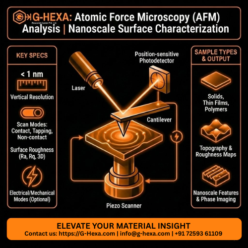
AFM Measurements with Industrial Performance

Many failure mechanisms originate at surfaces—roughness variation, adhesion loss, localized stiffness changes, or nanoscale wear. AFM enables direct correlation between surface physics and real-world reliability, offering insight beyond visual microscopy.

Advanced AFM Capabilities

Our Atomic Force Microscopy (AFM) platform delivers nanometer-scale surface characterization with exceptional spatial resolution. We enable topography mapping, roughness quantification, phase imaging, mechanical property evaluation, and nanoscale electrical or magnetic measurements across diverse material systems. From thin films and coatings to polymers, semiconductors, and advanced alloys, our AFM capabilities provide precise surface intelligence critical to performance-driven industries.

Topography Mapping

Sub-nanometer resolution surface profiling in contact and tapping modes.

Mechanical Property Mapping

Quantitative modulus, stiffness, and viscoelastic response measurement.

Adhesion & Friction Analysis

Nanoscale force interaction for tribological and coating evaluation.

Electrical & Magnetic Modes

Conductive AFM, KPFM, and MFM for multifunctional materials.

Expert Sample Preparation & Measurement Strategy

Reliable AFM results begin with disciplined sample preparation and a clearly defined measurement strategy. We tailor mounting, cleaning, surface conditioning, and environmental controls to the specific material system—ensuring minimal artifacts and maximum signal integrity.

Manufacturing–Surface Correlation

Surface condition directly influences adhesion, friction, fatigue life, conductivity, and coating integrity. We correlate processing parameters—such as deposition conditions, machining variables, polishing techniques, and thermal treatments—with measurable surface morphology and nanoscale property variations. This structured analysis helps industries optimize manufacturing workflows while maintaining consistency, durability, and functional performance.
Material DomainAFM InsightOptimization Impact
Polymers & ElastomersLocal stiffness and phase contrastImproved durability and formulation control
CoatingsRoughness, adhesion, wear tracksEnhanced lifetime and adhesion reliability
SemiconductorsSurface defects and electrical potentialYield improvement and device stability

Trained Interpretation, Actionable Insight

AFM data requires expert interpretation to translate nanoscale contrast into meaningful engineering conclusions. Our specialists combine materials science expertise with advanced image processing and quantitative analysis to ensure reliable roughness metrics, phase differentiation, and property mapping. The result is clear, defensible insight that supports quality control, R&D validation, and high-precision industrial decision-making.

Early Surface Degradation Detection

Identify wear, delamination, or plastic deformation at nanoscale.

Root Cause Surface Analysis

Link surface anomalies directly to process or material variables.

Rapid Feedback Loop

Accelerated optimization through quantitative surface metrics.

From Surface Science to Next-Generation Materials

AFM data informs smarter material design—engineered surfaces, functional coatings, and interfaces tuned for performance, reliability, and longevity in demanding industrial environments. Surface phenomena often define real-world material behavior. Through rigorous AFM analysis, we uncover nanoscale interactions that influence bonding strength, wear resistance, thin-film stability, and device efficiency. These insights extend beyond diagnostics—informing smarter material design, improved coatings, and the development of next-generation functional systems engineered for reliability and performance.

Focused Ion Beam (FIB) — Precision Access to Hidden Structures

Focused Ion Beam technology enables controlled, site-specific micromachining at the nanometer scale—unlocking subsurface features that define material performance. At G-Hexa, we use FIB not only as a preparation tool, but as a strategic investigative instrument. From high-accuracy cross-sectioning and TEM lamella preparation to defect isolation and interface analysis, our approach connects microscopic structure with manufacturing reality. By combining precision milling with deep materials expertise, we transform hidden microstructural evidence into reliable engineering decisions.

Surface Intelligence for Engineering Decisions

Share your challenge. We’ll configure an AFM strategy that converts nanoscale forces into actionable outcomes.