

Electron Backscatter Diffraction (EBSD) Analysis
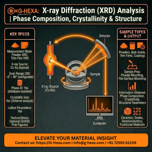
| Parameter | Specification |
|---|---|
| Technique | Electron Backscatter Diffraction (EBSD) |
| Operating Platform | FESEM-based EBSD system |
| Spatial Resolution | ~20–50 nm (material and setup dependent) |
| Angular Resolution | ~0.5° |
| Mapping Modes | Orientation mapping, phase mapping |
| Grain Analysis | Grain size, grain boundary character |
| Texture Analysis | Pole figures, inverse pole figures |
| Phase Discrimination | Yes (crystalline phases) |
| Sample Type | Metals, alloys, ceramics, crystalline materials |
| Sample Surface | Highly polished, strain-free surface required |
| Sample Preparation | Precision grinding, polishing, vibratory polishing |
| Information Obtained | Grain orientation, texture, phase distribution |
| Typical Use Cases | Metallurgy, ceramics, thin films, failure analysis |
Payment. Payment upon receipt of goods, Payment by card in the department, Google Pay, Online card, -5% discount in case of payment
Warranty. The Consumer Protection Act does not provide for the return of this product of proper quality.
Description
Advanced Electron Backscatter Diffraction service for crystallographic orientation, grain structure, and phase mapping of materials at the microscale. EBSD enables quantitative correlation between microstructure, texture, and material performance, particularly in polycrystalline and engineered materials.
Key Applications
-
Grain size and grain boundary analysis
-
Crystallographic orientation and texture mapping
-
Phase identification and phase distribution
-
Deformation, recrystallization, and failure analysis
-
Process optimization and quality assessment
Specifications
| Parameter | Specification |
|---|---|
| Technique | Electron Backscatter Diffraction (EBSD) |
| Operating Platform | FESEM-based EBSD system |
| Spatial Resolution | ~20–50 nm (material and setup dependent) |
| Angular Resolution | ~0.5° |
| Mapping Modes | Orientation mapping, phase mapping |
| Grain Analysis | Grain size, grain boundary character |
| Texture Analysis | Pole figures, inverse pole figures |
| Phase Discrimination | Yes (crystalline phases) |
| Sample Type | Metals, alloys, ceramics, crystalline materials |
| Sample Surface | Highly polished, strain-free surface required |
| Sample Preparation | Precision grinding, polishing, vibratory polishing |
| Information Obtained | Grain orientation, texture, phase distribution |
| Typical Use Cases | Metallurgy, ceramics, thin films, failure analysis |
Sample Preparation Support
-
EBSD-specific mechanical and vibratory polishing
-
Damage and deformation layer removal
-
Conductive coating guidance (if required)
-
Surface quality validation prior to mapping
-
(EBSD data quality is critically dependent on surface preparation and strain-free conditions.)
Deliverables
-
Orientation maps and phase maps
-
Grain size and grain boundary statistics
-
Texture plots (pole figures, IPFs)
-
Indexed EBSD datasets
-
Expert interpretation linked to processing and performance
Who Should Use This Service
-
Metallurgy and materials engineering teams
-
Ceramic and crystalline material researchers
-
Failure analysis and deformation studies
-
Industrial process development groups
Important Note
EBSD is sensitive to surface damage and crystallinity.
Amorphous materials or poorly prepared surfaces may not yield indexable patterns and may require complementary techniques such as TEM or XRD.

Reviews
There are no reviews yet.