
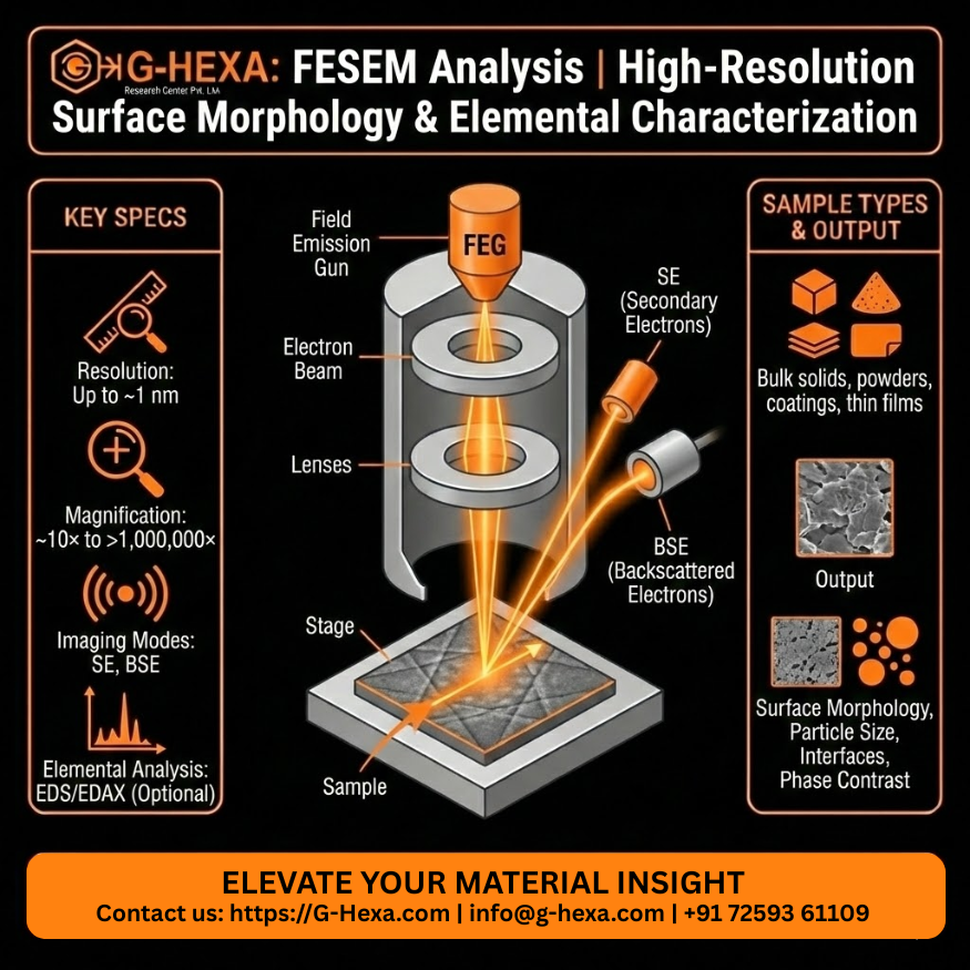
Field Emission Scanning Electron Microscopy (FESEM) Analysis
| Parameter | Specification |
|---|---|
| Technique | Field Emission Scanning Electron Microscopy (FESEM) |
| Resolution | Up to ~1 nm (instrument-dependent) |
| Magnification Range | ~10× to >1,000,000× |
| Accelerating Voltage | 0.5 – 30 kV |
| Imaging Modes | Secondary Electron (SE), Backscattered Electron (BSE) |
| Elemental Analysis | EDS / EDAX (optional) |
| Sample Type | Bulk solids, powders, coatings, thin films |
| Sample Conductivity | Conductive or non-conductive (coating supported) |
| Sample Preparation | Mounting, coating, cross-sectioning (optional) |
| Information Obtained | Surface morphology, particle size, interfaces, phase contrast |
| Typical Use Cases | Failure analysis, coating evaluation, semiconductor inspection |
Payment. Payment upon receipt of goods, Payment by card in the department, Google Pay, Online card, -5% discount in case of payment
Warranty. The Consumer Protection Act does not provide for the return of this product of proper quality.
Description
Advanced characterization service for high-resolution structural and compositional analysis of materials at micro- to atomic-scale, enabling reliable correlation between structure, interface, and performance.
Key Applications & Uses
- Failure analysis
- Interface and morphology evaluation
- Nanostructure and thin-film analysis
- Semiconductor and advanced material validation
Specifications
| Parameter | Specification |
|---|---|
| Technique | Field Emission Scanning Electron Microscopy (FESEM) |
| Resolution | Up to ~1 nm (instrument-dependent) |
| Magnification Range | ~10× to >1,000,000× |
| Accelerating Voltage | 0.5 – 30 kV |
| Imaging Modes | Secondary Electron (SE), Backscattered Electron (BSE) |
| Elemental Analysis | EDS / EDAX (optional) |
| Sample Type | Bulk solids, powders, coatings, thin films |
| Sample Conductivity | Conductive or non-conductive (coating supported) |
| Sample Preparation | Mounting, coating, cross-sectioning (optional) |
| Information Obtained | Surface morphology, particle size, interfaces, phase contrast |
| Typical Use Cases | Failure analysis, coating evaluation, semiconductor inspection |

Reviews
There are no reviews yet.