When light cannot see, electrons reveal. G-Hexa’s TEM capabilities bridge atomic-scale insights to industrial transformation — revealing dislocations, interfaces, and lattice perfection in real materials.
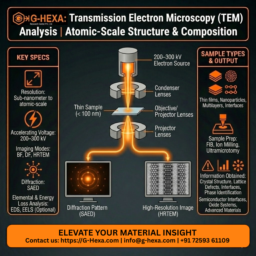
Transmission Electron Microscopy (TEM) visualizes the internal structure of matter down to individual atomic columns. With bright-field, dark-field, HRTEM, SAED, STEM-EDS, and EELS, it reveals crystal order, defects, and chemistry with sub-ångström precision. At G-Hexa, we use TEM not merely for imaging — but for decoding how atoms organize, react, and fail.
Resolution
Better than 1 Å — visualize atomic lattices and interfaces.
Diffraction & Phase Analysis
SAED pattern indexing for crystal identification and strain mapping.
STEM-EDS & EELS
Elemental and bonding analysis at atomic scale for interface chemistry.
Preparation and Characterization Challenges
TEM is both a precision craft and a scientific dialogue — demanding mastery over sample thinning, ion milling, and beam-matter interpretation. Accuracy depends not only on equipment but on deep material understanding.
Preparation Expertise
Electron-transparent specimens (<100 nm) without stress or amorphization.
FIB lift-out preserving interfaces and multilayers.
Ion-milling optimization to prevent redeposition or ion damage.
Contamination-free transfer for graphene and hybrid systems.
Interpretation Skill
Accurate SAED indexing and crystallography reasoning.
Understanding phase contrast and imaging conditions in HRTEM.
Managing beam sensitivity and drift in nano-hybrids.
Integrating EELS/EFTEM for oxidation-state and bonding insight.
At G-Hexa, trained analysts merge atomic imaging with scientific reasoning, ensuring that every lattice and diffraction spot becomes a clue to process history, not an artefact.
Atomic Insight ↔ Industrial Correlation
Every process leaves atomic footprints. TEM connects nanoscale defects and precipitates with macroscopic performance — guiding process tuning and material redesign.
Adjust synthesis to enhance load transfer and conductivity
Semiconductors
Interface traps, stacking faults, amorphous/crystalline zones
Improve epitaxial growth and reliability of devices
Vision — Atomic Intelligence for Industry
G-Hexa believes that the smallest scales hold the largest answers. Through disciplined TEM analysis and interpretive expertise, we help industries translate atomic-level evidence into process innovation.
“In TEM, clarity is not a function of resolution — it is a function of understanding.”
Vision — Atomic Intelligence for Industry
G-Hexa believes that the smallest scales hold the largest answers. Through disciplined TEM analysis and interpretive expertise, we help industries translate atomic-level evidence into process innovation.